


Perhaps the name ASML doesn't ring a bell, yet this Dutch company is an irreplaceable pillar in the global technology industry. We're talking about a true global powerhouse, silent but potent, playing a crucial role in the production of semiconductors, the "brains" of every electronic device.
Understanding the Semiconductor Value Chain: An Essential Approach
Before we delve into the heart of ASML, it's essential to explore the semiconductor value chain. This sector is structured into various types of companies, each with a well-defined role:
Fab Companies (Foundry): These are the foundries, the actual factories that handle the physical production of semiconductors. They are equipped with state-of-the-art machinery to transform raw materials into functional chips.
Fabless Companies: Conversely, fabless companies specialize in chip design and development, but choose to outsource production to an external foundry. A striking example of a fabless company is Nvidia, a name familiar to everyone in the field of artificial intelligence. Nvidia designs its chips, but then entrusts their production to TSMC (Taiwan Semiconductor Manufacturing Company), the most important and technologically advanced foundry in the world. To give you an idea of its relevance, over 60% of global chips are produced by TSMC.
Software and Architectures: The Pillars of Chip Design
The value chain, seemingly complex, turns out to be more linear than one might imagine. Before a chip is physically produced, another category of crucial players comes into play:
Software Companies (EDA - Electronic Design Automation): Companies like Synopsys and Cadence develop the essential software for chip design and testing. Nvidia, for example, before sending a production order to TSMC, must design and validate the feasibility of its chips using these advanced software tools. Their importance in the semiconductor value chain is, therefore, undeniable.
Architecture Companies: Companies like ARM are dedicated to defining the architecture upon which the chip will be designed. This architecture is the fundamental basis on which designs from companies like Nvidia, AMD, and many others are developed.
From Design to Production: ASML's Invaluable Role
Once the design and testing phase is complete, fabless companies turn to specialized foundries, often located in Taiwan or other high-tech regions, to begin production. But how do these foundries produce microchips? The answer is simple: thanks to ASML's machinery (and its few competitors).
ASML is a leader in the production of lithography systems, extremely sophisticated machines that use ultraviolet light to "print" microscopic circuits onto silicon wafers. These systems are so precise that they allow for the creation of chips with geometries down to 2 nanometers, paving the way for ever-increasing performance and computing capabilities. Without ASML's technologies, the current level of innovation in the semiconductor sector would be unthinkable.
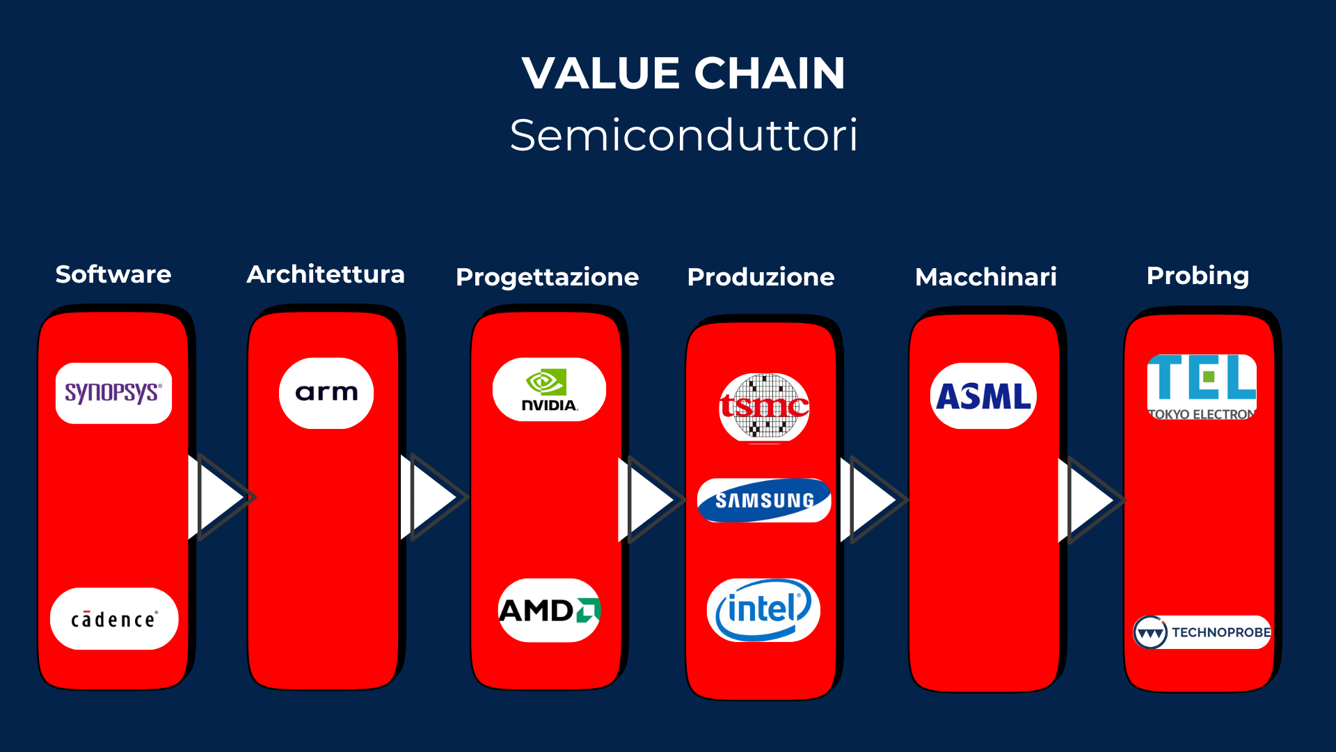
Probing: Ensuring Quality in Semiconductors
Finally, in the sophisticated semiconductor value chain, we find probing companies. Their role is simple but crucial: to verify that chip production has been successful and defect-free. A notable example in this field is Technoprobe, an Italian company that boasts a direct collaboration with industry giants like TSMC. Thanks to their advanced testing systems, they ensure that only perfectly functioning chips reach the market.
Our Journey into the World of ASML: Starting with History
Now that we understand the general industry context, we can delve into our adventure in the world of ASML. As with every company analysis we present, we'll begin with an in-depth look at the company's history. We firmly believe that understanding a company's evolutionary journey allows for a deeper and more complete comprehension of its value and current market position.
In this article, you'll find:
The History of ASML: From a Leaky Shed to Global Dominance
The Origins: A Joint Venture Born Out of Necessity (1984)
ASML's story began in rather humble circumstances in 1984. In an era of rapid growth for the semiconductor industry, with ever-increasing production complexity, the colossal Dutch electronics company Philips and the chip machinery manufacturer ASM International decided to join forces. Born as a joint venture, their goal was to develop cutting-edge lithography systems capable of meeting the demands of a rapidly expanding market. Their initial purpose? To commercialize the PAS 2000, an innovative "wafer stepper" developed by Philips itself.
The Road to Independence and Unstoppable Growth
Initially, ASML operated with extremely limited resources; in fact, it's rumored they even started from a "leaky shed." Despite these unfavorable conditions, a deep belief in innovation and research & development allowed ASML to make rapid and significant progress. In 1988, the company took a pivotal step, becoming fully independent from Philips and ASM International, yet retaining the name ASML, which officially became its designation.
The Rise in the Semiconductor Sector: A Constant Path of Innovation
From that moment on, ASML continued to innovate, developing increasingly sophisticated lithography technologies and establishing itself as the undisputed leader in the sector:
1990s and 2000s: ASML solidified its position thanks to its deep ultraviolet (DUV) lithography systems. These machines enabled the production of chips with ever-smaller features, pushing the limits of miniaturization.
2001: A crucial year saw ASML acquire Silicon Valley Group (SVG), a significant competitor. This strategic move granted ASML access to important intellectual property and EUV licenses, fundamental for the development of future technologies.
2012: The year of a momentous breakthrough. ASML introduced its first extreme ultraviolet (EUV) lithography system. This revolutionary technology made it possible to "print" circuits with nanometer dimensions, allowing the company to continue pushing the boundaries of Moore's Law (which predicts the doubling of microchip power every two years). Today, ASML holds virtually a monopoly on this EUV technology, making it an indispensable supplier for the world's largest chip manufacturers, such as TSMC, Intel, and Samsung.
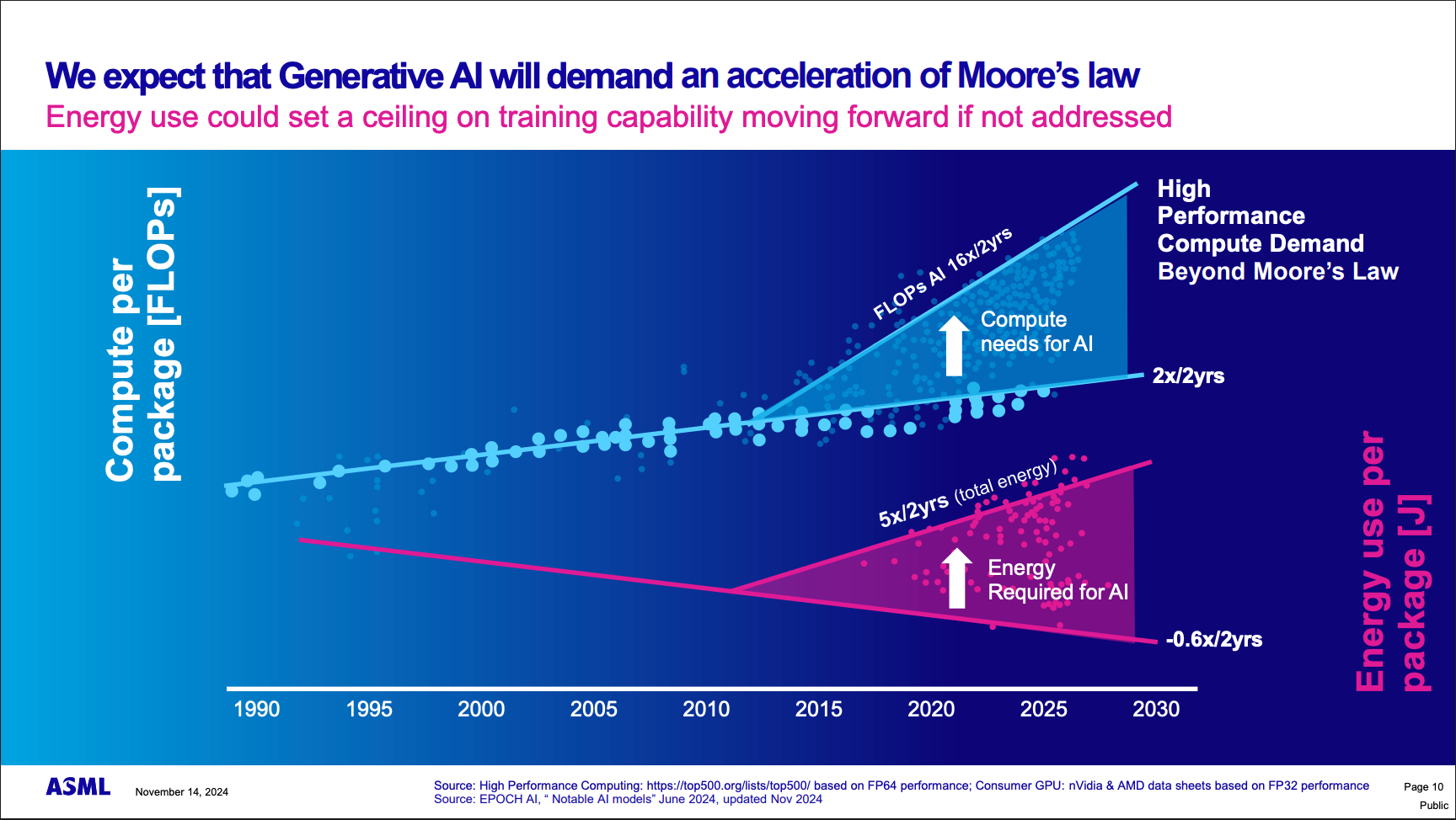
This historical progression shows how ASML transformed from humble beginnings to an undisputed leadership position, becoming a fundamental pillar of the entire technology industry. However, technological evolution doesn't stop, and with the advent of Generative Artificial Intelligence, the demand for computing power is accelerating at a rate that challenges even the most optimistic Moore's Law predictions. As illustrated in the following graph, this acceleration presents significant challenges, particularly regarding energy consumption, which could soon become the main limit to AI model training capacity if not addressed with innovative solutions.
What Does ASML Do? Photolithography at the Heart of Chips
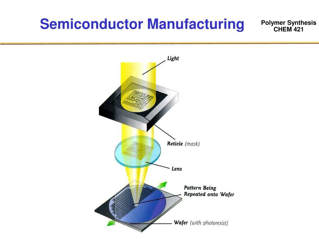
ASML specializes in photolithography, an extremely precise printing process that uses laser beams and ultraviolet light to create the chips that power our technology.
Founded in 1984 from the merger of ASM and Philips, ASML was born with the ambitious goal of developing advanced methodologies in the field of photolithographic printing. The initial intent was to refine a technique crucial for U.S. military needs.
ASML's Core: Photolithography and the Art of Chipmaking
The technology underpinning current chip production, and thus the heart of ASML's operations, is photolithography. It's thanks to this complex procedure that microscopic circuits can be "etched" onto silicon wafers, making possible the creation of increasingly powerful and compact semiconductors.
This allows them to miniaturize patterns and transfer them onto silicon wafers, the primary material for today's chips. The idea was revolutionary: if a microscope can enlarge objects, inverted lenses can shrink them.
It simply works like this:
You coat the wafer with a chemical substance that becomes insoluble when exposed to light.
By inverting the microscope lenses, a smaller, rather than larger, image is created on the other side.
The desired pattern is placed under the microscope.
Light emanates from the other side of the microscope.
A smaller version of the pattern is reflected onto the wafer, and that part of the wafer becomes insoluble.
The soluble part is washed away to extract the pattern.
Business Profile
In essence, ASML designs, manufactures, and markets highly advanced photolithography systems. These cutting-edge machines are essential for "printing" complex chip patterns onto silicon wafers. ASML's clients are the world's largest semiconductor manufacturers, such as TSMC, Samsung, and Intel, who use these machines to transform the designs of "fabless" companies (like Qualcomm, Nvidia, and AMD, which we discussed in the previous value chain) into physical products.
The Microscopic Detail That Makes the Difference: Why Light is the Key to Our Chips
Imagine a microchip as a miniature metropolis, with a dense network of roads, buildings, and complex infrastructure. To "build" these nanometer-scale cities, the semiconductor industry relies on a technique called photolithography. In simple terms, it's a process that uses an extremely precise projector to "print" circuit designs, layer by layer, onto a silicon wafer.
The crucial point—and this is where the central role of the Dutch giant ASML comes into play—is that the minimum size of the details we can etch onto a chip is directly related to the wavelength of the light used. Think of writing with a marker: if the tip is thick, the details will be coarse; if the tip is fine, you can draw with precision. The same logic applies to light: the thinner its "tip" (the wavelength), the smaller and more defined the details we can impress.
In the early 1990s, the most advanced photolithography machines employed deep ultraviolet (DUV) light, with a wavelength of 193 nanometers. A tiny value, certainly, but not enough for the industry's miniaturization ambitions. Already in 1991, brilliant scientists at Bell Labs posed a challenge: what would happen if we could use light with a wavelength of only 13.8 nanometers?
The initial idea was to pivot to X-rays, known for their incredibly short wavelengths, promising infinitesimal details. The problem, however, was their "elusive" nature: X-rays cannot be easily focused with traditional lenses, making their management a true technological nightmare.
It was in this context that the winning intuition directed research towards extreme ultraviolet (EUV) light. With its 13.8 nanometers, EUV sits right on the border between ultraviolet and "softer" X-rays, offering a brilliant compromise: precision almost equal to that of X-rays, but with the possibility, albeit extremely complex, of being managed and focused.
This was a titanic challenge, a true technological "leap of faith" that would require years of intense research and development, with success far from guaranteed. Yet, in 1999, ASML made a bold decision: to invest massively in the development of these EUV machines. A gamble that, as we know today, would forever revolutionize the face of the semiconductor industry, positioning ASML as the undisputed monopolist of a technology that is literally the key to the chips of the future.
ASML's Audacious Bet: Building an Ecosystem from Scratch
We've seen how EUV light was the key to unlocking extreme chip miniaturization. But the story doesn't end there. In fact, it's precisely at this point that ASML's true genius (and tenacity) powerfully emerges.
In 1999, when ASML decided to throw caution to the wind and invest billions in EUV technology, it wasn't just a brilliant idea. It was about confronting a harsh reality: many of the crucial components needed to build these futuristic machines simply didn't exist. ASML found itself in the position of having to build not just the machine, but the entire supplier ecosystem from the ground up.
This colossal undertaking is reflected in the development timeline: it took a full 18 years to deliver the first commercial EUV lithography machine to Samsung. An endeavor that testifies to ASML's incredible vision and perseverance in pursuing a goal that once seemed unattainable.
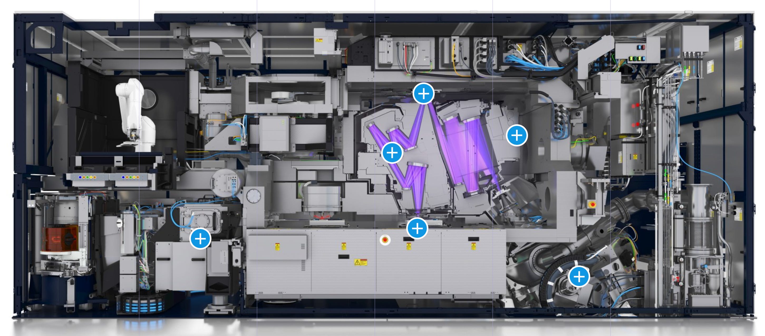
The machine pictured above is an EUV (Extremely Ultraviolet) system, ASML's flagship product and the foundation of its industry monopoly. Costing over $300 million, this machine is an engineering masterpiece, comprising seven main blocks. Each "block" is manufactured in different parts of the world, then shipped to Veldhoven, Netherlands, for assembly and rigorous testing.
Once testing is complete, logistics become a monumental undertaking: shipping requires 20 trucks and no fewer than 3 Boeing 747 cargo planes, necessitating a new disassembly of the machinery for transport.
Unlike EUV systems, ASML's DUV (Deep Ultraviolet) machines face greater competition from other manufacturers. However, it's crucial to emphasize that with current technological advancements, EUV machines will be increasingly in demand, as they enable the production of chips with geometries down to 2 nanometers, pushing the limits of semiconductor capabilities.
ASML's Ecosystem: An Unprecedented Vision
Imagine wanting to build a spaceship, only to discover that no one produces the warp engines or dilithium crystals you need. This was ASML's situation at the crucial moment of EUV development. Potential suppliers hesitated, finding the endeavor too risky, difficult, and expensive.
But ASML didn't give up. It did what very few companies would have dared: it built its own ecosystem, uniting suppliers and innovation into a single, powerful network.
Here are some examples of their incredible dedication and foresight:
The Pharaonic Investment in Zeiss: To focus light as extreme as EUV, mirrors of unimaginable precision were needed—the smoothest ever created by humans. Since no one was producing them, ASML didn't just ask or plead. It decided to invest a whopping $1 billion in Zeiss, the German optics giant, to enable them to develop these "science fiction" mirrors. A financial commitment that testifies to unwavering confidence and the realization that without that key piece, the entire technological puzzle would be meaningless.
The Network of 5,000 Suppliers: The investment in Zeiss was not an isolated case. ASML wove an incredibly dense network, developing deep ties and joint research and development processes with over 5,000 suppliers worldwide. Instead of simply buying components, ASML co-created, pushing entire industries to develop the specific technologies and materials required by its EUV machines. They were true partners on a journey into the unknown.
Acquisition of the "Doubtful": And what if a key supplier wasn't up to par or didn't share the same audacious vision? ASML had no qualms. It directly acquired companies it deemed too critical or unreliable to be left to chance, ensuring full control over essential components:
Brion Technologies (2007, $270 million): Acquired to optimize and verify the "masks," which are the patterns projected onto the chips.
Cymer (2012, $2.5 billion): A gigantic move to secure the production of EUV light sources, the true "beating heart" of the machines. A fundamental company that could not be left outside direct control.
Hermes Microvision (2016, $3.1 billion): Acquired to ensure quality in defect identification, a crucial step for production efficiency and chip yield.
This aggressive and visionary strategy not only allowed ASML to overcome seemingly insurmountable obstacles, but it also cemented its position as a monopolist in a vital sector. They didn't just innovate their own product; they rebuilt the entire supply chain around their vision. And that's how a Dutch company became the nerve center of global technological production.
ASML's Unsurpassable Competitive Advantage
ASML's machines, particularly its EUV systems, cannot simply be replicated through reverse engineering. Their competitive advantage is rooted in a unique set of factors:
Unique Supplier Relationships: No one else possesses the same level of relationships with the 5,000 suppliers and the joint research and development processes that ASML has cultivated over decades. Even if a competitor managed to identify all the components, placing an order would be nearly impossible, as all key production capacities for these components are already absorbed and dedicated to ASML.
Difficulty in Internal Integration: Sourcing internally the complex components that ASML has helped develop and integrate is an almost impossible feat for a new entrant.
Dominant Market Share: While holding a 100% market share in EUV machines, ASML also boasts over 90% of the deep ultraviolet (DUVL) lithography market, the preceding technology.
Overall, ASML's competitive moat is rock-solid. It is arguably the most robust one can observe in the semiconductor industry, even harder to overcome than that of giants like TSMC.
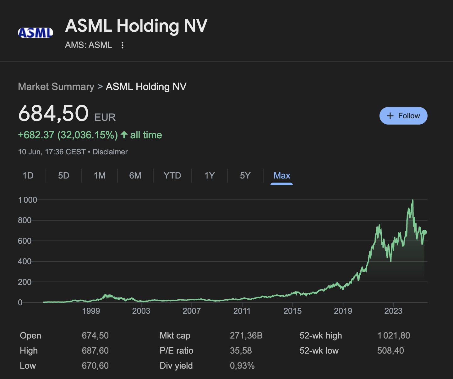
And indeed, ASML has delivered a monstrous return to its shareholders since its IPO, despite having fallen 35% from its all-time highs, partly due to tariffs imposed by Trump. This turbulence shouldn't concern us, as it will be temporary.
Market Profile
ASML's market profile is currently interesting, as the company is trading at attractive multiples, specifically below its historical average.
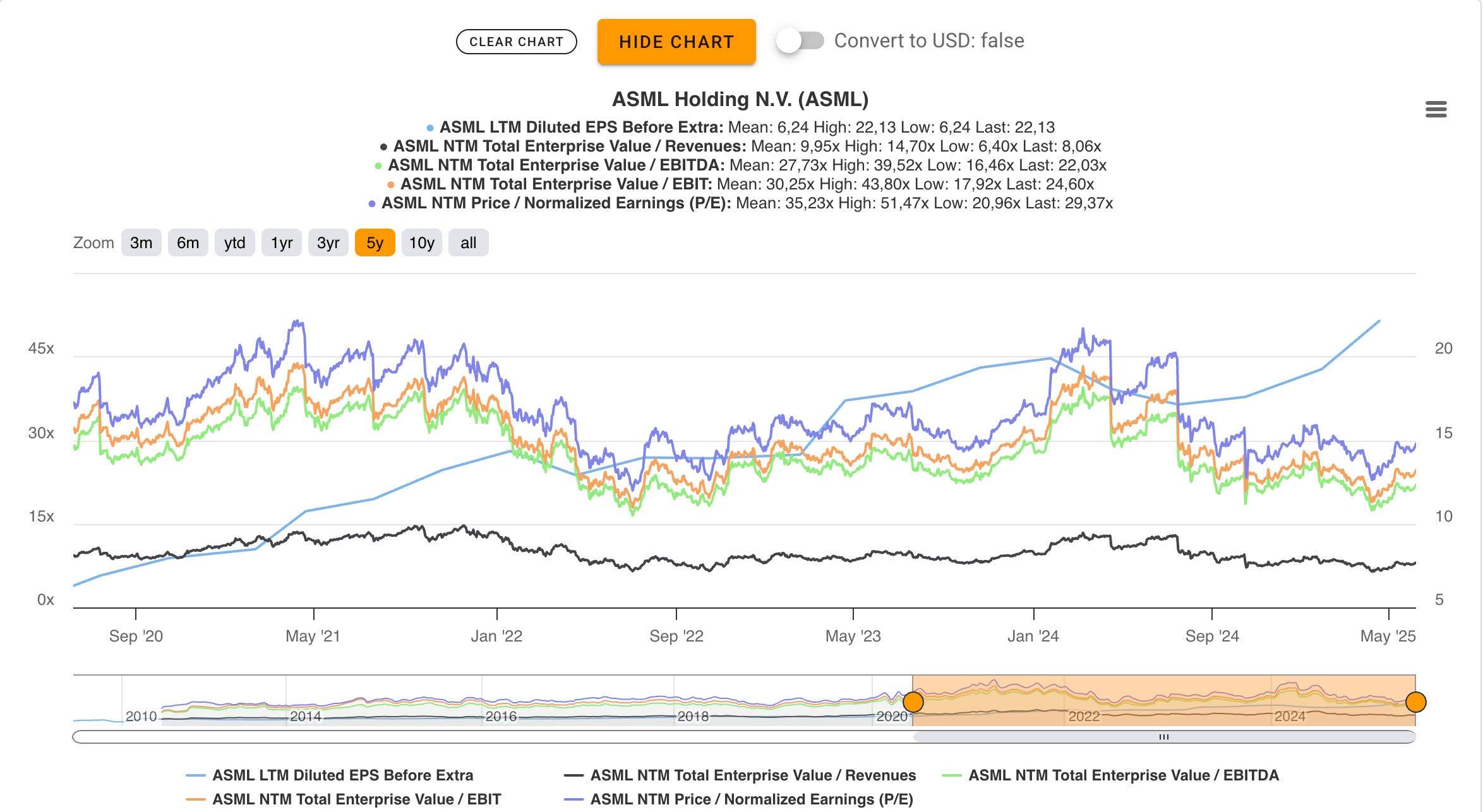
It's crucial to understand that ASML operates in a market context that can be defined as a quasi-monopoly. We emphasize "quasi" because, while ASML indisputably dominates certain niches, it also produces DUV (Deep Ultraviolet) machinery, for which there is some, albeit limited, competition.
As the graph below illustrates, ASML's stock is currently trading below its historical average. This observation provides an important perspective on its market valuation.
Despite potential turbulence related to external factors (like Trump's policies, mentioned in the latest Q1 2025 earnings call), ASML's management has confirmed the guidance provided during its 2022 Capital Markets Day. This ambitious yet realistic forecast indicates a 10% annual growth rate for the next ten years.
In light of this confirmation from management itself, we believe that analyst estimates regarding ASML can be considered particularly accurate. Furthermore, it's plausible to assume excellent margin control, which could see an increase of a few percentage points. This is possible thanks to the strong bargaining power the company enjoys, given its quasi-monopoly position in its key sector.
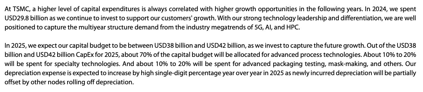
Considering TSMC's management forecasts, which predict a doubling of Artificial Intelligence (AI) related revenues in 2025, it's highly plausible that a significant portion of TSMC's Capex (capital expenditures) will directly translate into increased revenue for ASML.
This connection is strengthened by the fact that a large part of TSMC's production is now shifting towards chips with sub-7 and 10 nanometer technology nodes. We know that ASML's EUV (Extreme Ultraviolet) machinery, in which it holds a monopoly, is indispensable for producing these cutting-edge chips.
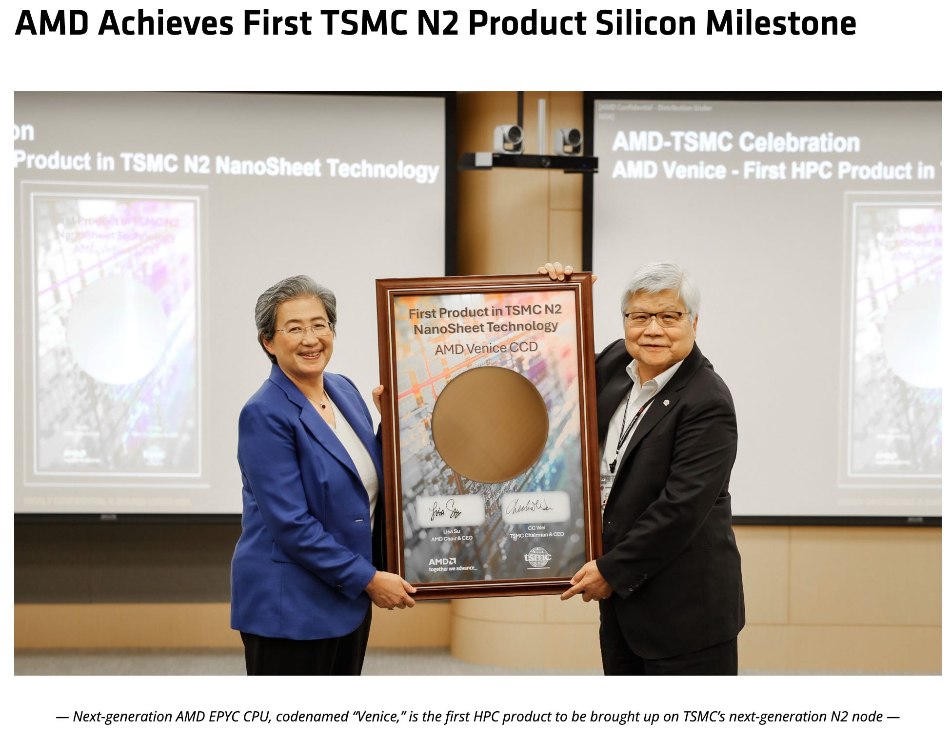
Furthermore, it's important to highlight that this year AMD has already produced its first 2-nanometer chip, made in collaboration with TSMC. This success further underscores the acceleration towards increasingly advanced production technologies, solidifying ASML's crucial position in the entire semiconductor value chain.
This scenario leads us to reflect deeply on the future of semiconductor manufacturing. The increasing technological complexity and the ever-higher demand for advanced chips will inevitably require a growing number of cutting-edge machines for their production.
Financial Profile
In light of our analysis, we can confirm that ASML has a clear path forward, with solid and lasting growth prospects. Most likely, the company will continue to generate excellent average returns for shareholders. As proof of this, over the last three years (2022-2023-2024), ASML has recorded an average ROE of 54%, an indicator of exceptional profitability and capital management.
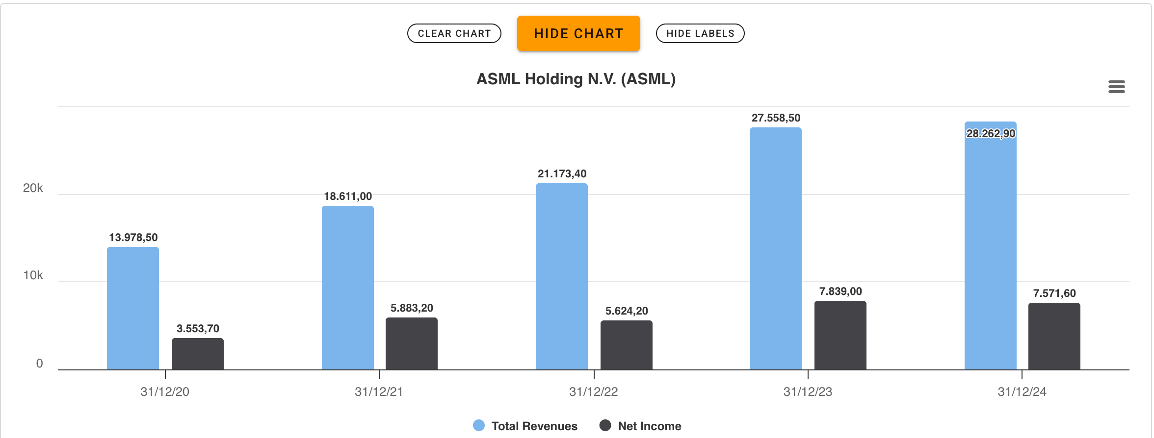
Analyzing ASML's financial profile reveals extremely robust revenue growth. In fact, over the past five years, revenues have doubled, increasing by 100%. This significant expansion has been accompanied by an even more marked increase in net income, which grew by 113% during the same period. These figures underscore ASML's ability to convert top-line growth into consistent profits for its investors.
These financial figures not only highlight robust growth but also allow us to appreciate ASML's operational consistency. The company demonstrates a remarkable ability to maintain high and reliable returns over time, a reassuring sign for investors.
From a financial perspective, the silent giant presents an extremely positive outlook in the ratio between its generated EBITDA (Earnings Before Interest, Taxes, Depreciation, and Amortization) and its total debt (i.e., long-term debt). This indicator is crucial for assessing the company's ability to repay its debts with operating cash flows, confirming a solid financial position.
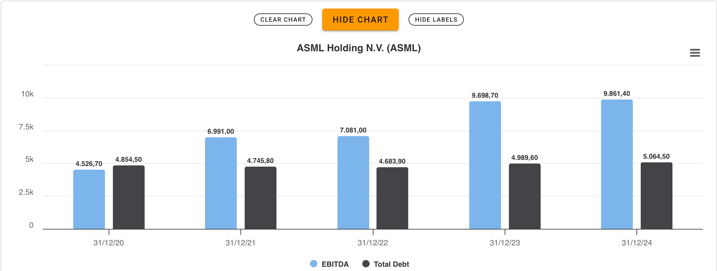
Observing the graph closely, it's evident that ASML is capable of extinguishing its entire debt in approximately six months, thanks to its generated EBITDA. In fact, as of December 31, 2024, the Net Debt/EBITDA ratio stood at -0.77. This value indicates a negative net financial position, which means the company holds a net cash position, with more available liquidity than debt.
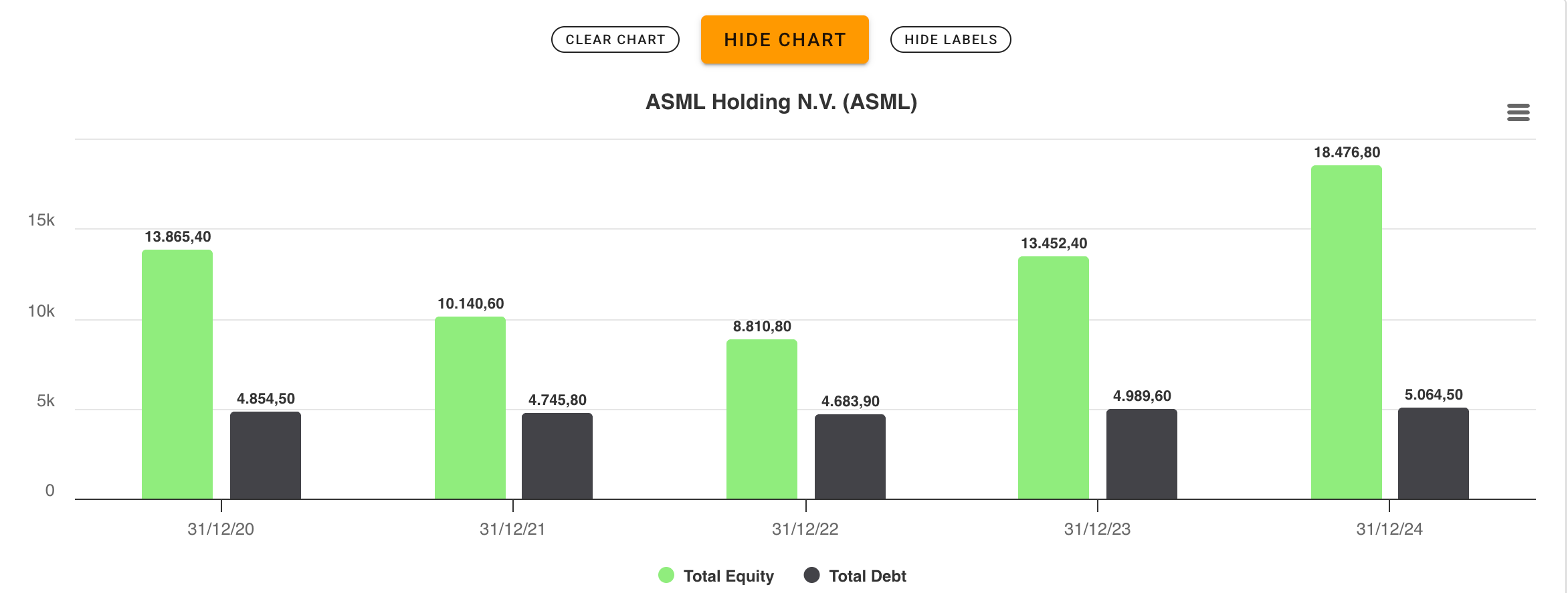
ASML's financial strength is further confirmed by its Total Debt/Equity ratio, which is 27.4%. This signifies that the company is primarily financed by shareholders' equity, rather than by debt.
This particular financial structure deserves deep reflection, especially considering that ASML produces extremely expensive machinery, with prices starting from $200 million and going upwards. A company with such a business model, if it didn't possess such strong technological advancement and broad bargaining power, would not be able to manage debt with such ease and maintain such a robust capital structure.
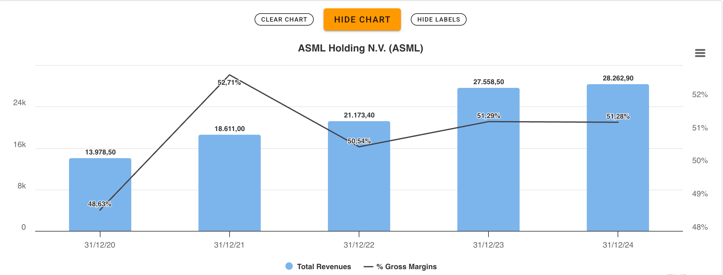
Margins: An Indicator of Bargaining Power
A crucial detail in ASML's financial analysis is its gross margin. As the graph illustrates, in 2022, due to high inflation, the company's gross margin saw a slight dip, only to resume its growth in subsequent years.
The guidance provided by management anticipates a further expansion of approximately 5 percentage points in gross margin by 2030. This figure is a clear symptom of ASML's strong bargaining power, as gross margin reflects efficiency in managing variable costs, not fixed ones. Maintaining such high percentages, especially for a complex manufacturing company like ASML, is no simple feat and testifies to its dominant position.
Final Assessments: ASML and the Future of AI
In light of everything we've analyzed so far, we can firmly state that ASML positions itself as a "quasi-monopolist" in its sector. This position is poised to strengthen further thanks to the powerful trend of Artificial Intelligence (AI), which will demand continuous and massive investments not only from Big Tech (in data centers) but also from governments and, consequently, from various semiconductor manufacturers.
For this trend of growth and innovation to continue relentlessly, ASML's machinery, particularly those equipped with its cutting-edge photolithography technology, are absolutely essential and irreplaceable.
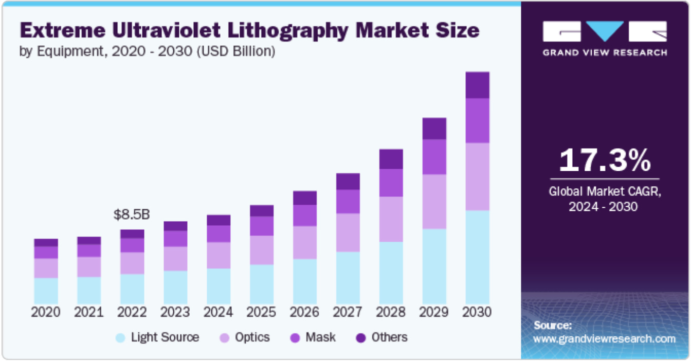
Let's now take a look at the industry's CAGR (Compound Annual Growth Rate) to better understand the expected growth dynamics:
ASML Value Projections and Target Price
Considering the strong estimated growth for the sector (as highlighted by the preceding CAGR) and ASML's dominant position, we've conducted an analysis to determine an intrinsic value that adequately reflects the potential of this company, which we believe is significantly undervalued.
Our projections are based on a long-term perspective and were calculated using the Discounted Cash Flow (DCF) model. This led us to define a target price of €1027 per share.
It's important to note that these projections could be "adjusted" if one of ASML's main customers, such as TSMC, were to increase orders due to a rise in its Capex Growth.
Technical Analysis of ASML: All-Time Highs, Corrections, and Accumulation Phase
ASML reached its all-time highs in July 2024, during a period when its multiples had surged to what were considered excessive valuations. Subsequently, the market initiated a bearish trend, seeking a return to the mean in terms of valuations.
After hitting its low on April 7, 2025, due to market turbulence (also related to Trump's statements), ASML attempted a very strong rebound but failed to break above the €675 per share threshold.
Currently, the stock is in an accumulation phase. It's precisely during this period that ASML's management is completing its €12 billion buyback program, which began in 2022. They're acquiring an average of €65 million per day, aiming to exhaust the remaining buyback authorization (approximately €6 billion left to purchase in 2025).
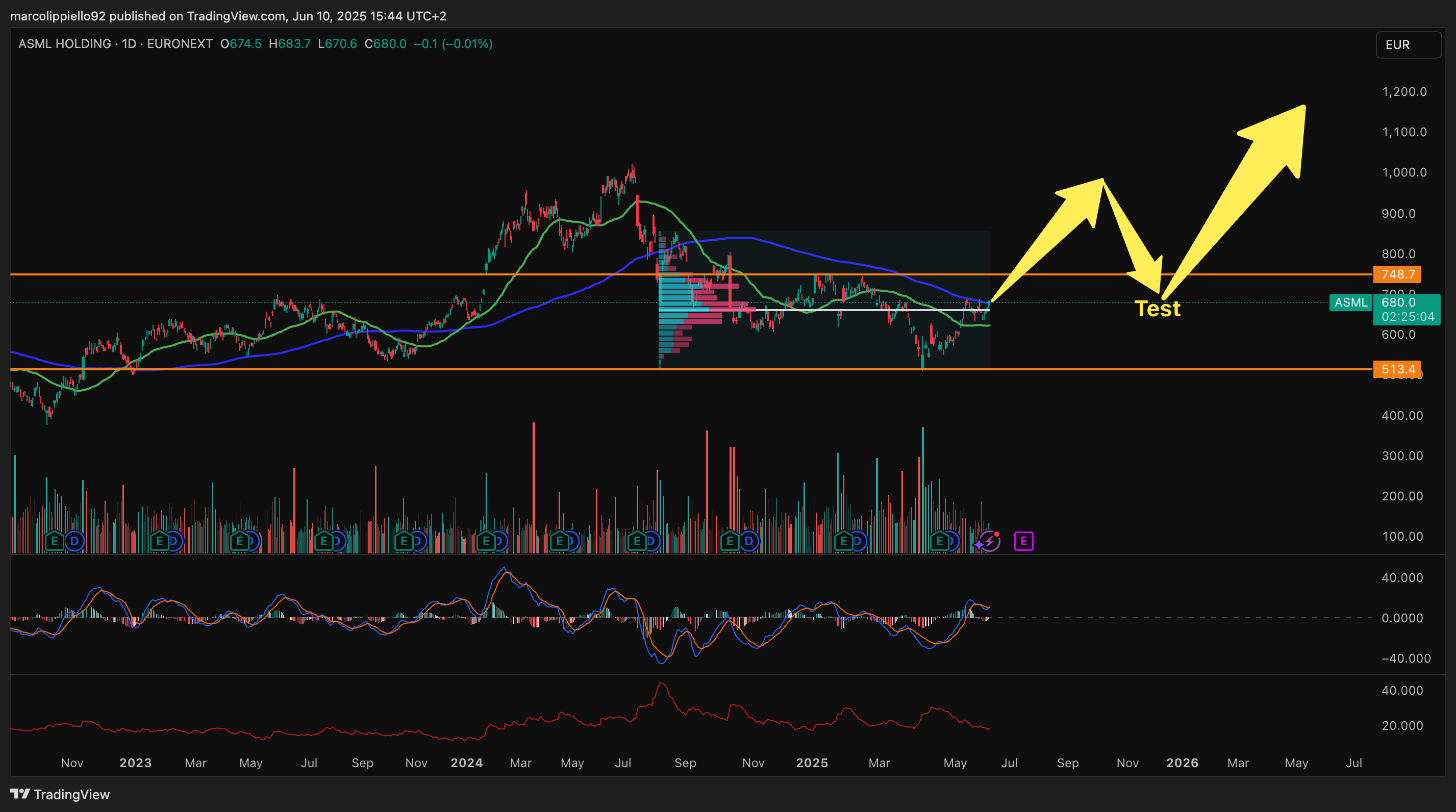
Considering the accumulation phase ASML is currently undergoing within the channel, we can assert that the bullish trend hasn't begun yet. To see a significant change in direction, we'll need to witness a test on the POC (Point of Control) once the price action breaks out of this accumulation phase. Until then, ASML's trend remains unchanged.
No one can precisely predict the duration of an accumulation phase; it could last days, weeks, or even months. The only certainty, based on our analysis, is that ASML, at current prices, is undervalued.
All opinions and viewpoints mentioned in this report constitute our judgments as of the date of writing and are subject to change at any time. The information contained herein is not intended as a primary basis for investment decisions and should not be construed as advice that meets the particular investment needs of any individual investor. Please remember that investing involves risks, including loss of principal, and past performance may not be indicative of future results. Equity Analysis, its members, officers, directors, and employees expressly disclaim all liability for actions taken based on all or part of the information contained in this writing.